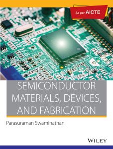
Semiconductor Materials, Devices, and Fabrication, As per AICTE
ISBN: 9788126508624
380 pages
For more information write to us at: acadmktg@wiley.com

Description
Semiconductor Materials, Devices, and Fabrication and the associated media content in the DVDs provide an understanding of the materials, devices, and processing techniques used in the current microelectronics industry. The 2 DVDs include 32 lectures, approximately an hour each. The lectures map onto the individual chapters in the book. The content is divided into three parts. Part I explains the basic physics behind semiconductor materials. Part II introduces electronic devices including optical devices. Part III discusses current manufacturing processes in the semiconductor industry, starting from wafer production to final integrated circuit development. The focus in this part is on industry challenges during miniaturization and methods to overcome these challenges.
Preface
About the Author
Part I – Semiconductor Materials
Chapter 1 Electronic Materials
1.1 Introduction
1.2 Molecular Orbital Formation
1.3 Molecular Orbitals in Extended Systems
1.4 Energy Bands in Metals
Chapter 2 Semiconductors: Introduction
2.1 Introduction
2.2 Band Formation in Semiconductors
2.3 Classification of Semiconductors
2.4 Electron Effective Mass
Chapter 3 Electron Statistics in a Solid
Learning Objectives
3.1 Density of States
3.2 Electron Occupation Probability
3.3 Density of States in Silver
3.4 Fermi Function versus Boltzmann Function
Chapter 4 Intrinsic Semiconductors
4.1 Introduction
4.2 Intrinsic Silicon
4.3 Conductivity Equation
4.4 Carrier Concentration in Semiconductors
4.5 Fermi Level Position in Intrinsic Semiconductors
4.6 Temperature Effect on ni
Chapter 5 Extrinsic Semiconductors
5.1 Introduction
5.2 Doping Types
5.3 Compensation Doping
5.4 Dopant Materials
5.5 Fermi Level in Extrinsic Semiconductors
5.6 Temperature Dependence of Carrier Concentration
5.7 Carrier Mobility
5.8 Degenerate Semiconductors
5.9 Amorphous Semiconductors
Part II – Devices
Chapter 6 Metal–Semiconductor Junctions
Learning Objectives
6.1 Metal–Metal Junctions
6.2 Schottky Junctions
6.3 Ohmic Junctions
Chapter 7 pn Junctions
Learning Objectives
7.1 Introduction
7.2 pn Junction
7.3 Calculation of Junction Parameters
7.4 Junction Potential versus Fermi Level Position
7.5 pn Junction Under Bias
7.6 Reverse Bias
7.7 Junction Breakdown
7.8 Heterojunctions
Chapter 8 Transistors
8.1 Introduction
8.2 Bipolar Junction Transistor
8.3 Junction Field-effect Transistor
8.4 Metal Oxide Semiconductor FET
8.5 MOS Band Structure
8.6 Role of Oxide Layer
Chapter 9 Light Semiconductor Interaction
9.1 Optical Absorption
9.2 Recombination and Carrier Lifetime
9.3 Continuity Equation
Chapter 10 LEDs and LASERs
10.1 Optical Emission
10.2 pn Junction-based LEDs
10.3 LED Materials
10.4 Solid-state LASERs
10.5 Device Structure
10.6 Specialty Lasers
Chapter 11 Photodetectors and Solar Cells
11.1 Photodetectors Working Principle
11.2 Types of Photodetectors
11.3 Solar Cell Basics
11.4 pn Junction Solar Cell
11.5 Solar Cell Materials and Efficiency
Part III – Fabrication
Chapter 12 Development of ICs
12.1 Introduction
12.2 Integrated Circuits
12.3 Device Miniaturization
12.4 Challenges in IC Manufacturing
12.5 IC Manufacturing Stages
Chapter 13 Silicon Wafer Manufacturing
13.1 Wafer Specification
13.2 Polysilicon Manufacture
13.3 Single Crystal Si Manufacture
13.4 Wafer Manufacturing
Chapter 14 Integrated Circuit Fabrication
14.1 Fabrication Overview
14.2 Layering
14.3 Patterning
14.4 Doping
14.5 Heat Treatment
14.6 MOSFET Fabrication
Chapter 15 Oxidation and Doping
15.1 Oxidation
15.2 Types of Oxidation Processes
15.2.1 Oxide Growth Model and Parameters
15.3 Oxide Furnaces
15.4 Doping Techniques
15.5 Thermal Diffusion
15.6 Ion Implantation
Chapter 16 Lithography
16.1 Introduction
16.2 Process Overview
16.3 Photoresists
16.4 Mask Making
16.5 Photoresist Application
16.6 Alignment and Exposure
16.7 Developing
16.8 Lithography Advances
Chapter 17 Etching and Deposition
17.1 Etching Basics
17.2 Wet Etching
17.3 Dry Etching
17.4 Deposition
Chapter 18 Metallization and Polishing
18.1 Metallization Basics
18.2 Metallization Materials
18.3 Metallization Techniques
18.4 Planarization
18.5 Copper Dual-Damascene Process
Chapter 19 IC Process Control
19.1 Process Evaluation
19.2 Electrical Measurements
19.3 Thickness Measurement
19.4 Defect Detection
19.5 Process Evaluation
19.6 Yield Models and Fabrication Costs
19.7 Clean Room Contamination
19.8 Clean Room Design and Materials
Chapter 20 IC Architecture and Packaging
20.1 Integrated Circuit Components
20.2 MEMS Systems
20.3 Silicon Micro-architecture
20.4 Packaging
Summary
Practice Questions
Answers
Bibliography
Index

